Business
We possess assembly and etching equipment that is used in semiconductor
and display process using plasma.
Plasma Application Technology
We possess assembly and etching equipment that is used in semiconductor and display process using plasma.
- Semiconductor Area: Plasma Assembly(Sputter) and Plama Process(Descum)
- Display Area: Back plane and Plasma desposition equipment for TFE (PEALD, PECVD)
- Sputter System
- Descum System
- Thin Film Encapsulation
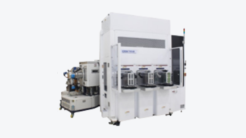
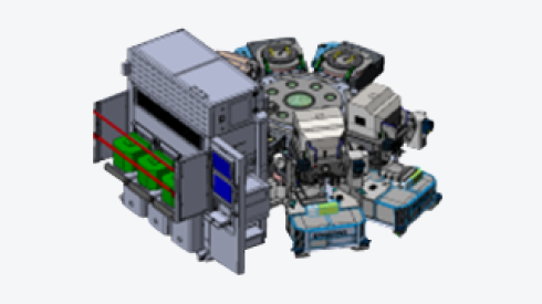
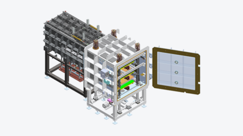
Sputter System
KORONA™ PVD600_ Advanced Package Process
- Semiconductor Advanced Package Sputter
- Following the high capacity, faster, and smaller trends of semiconductor devices, semiconductor Packaging technology has also been developed from the
previous Wire bonding to Flip Chip, and recently to FOWLP/FOPLP and 3D Packaging. - As the semiconductor Packaging technology is being developed, we at AP Systems, are providing client companies with Sputtering equipment for manufacturing
relevant metal films (CPB,UBM and RDL)
Technology
- Substrate Shift Detection & Align Technology when entering into each
chamber - ESC technology for low temperature (-20℃) to secure optimal process
(@ Preclearing & Process) - Multi Plate Heating System composition technology for Long Term Degas Time
(at least 30mins.) & High Temp. Uniformity
- Plasma Etching Chamber in the CCP form applied in Situ Pasting for the
Lower Particles - Magnetron Sputtering Source technology for High Film Quality and Film
Uniformity (Magnetron Scan & Tilt for FOPLP) - Verified Software Tool (Easy ClusterTM) operating technology applied to various semiconductor equipment
Features
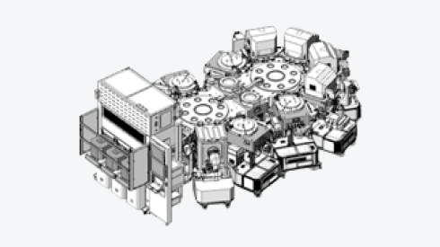
PVD600: CPB & FOWLP
- Board Information: Diameter 300mm including EMC (Epoxy Molding Compound)
- EFEM, 2LoadLock, Octagonal Transfer Chamber, 2Multi_Degas Chamber,
2Pre-Cleaning Chamber (CCP) & 2Process Module
PVD600_R450: FOPLP
- Board Information: Rectangular (Approximately 400 x 500mm) type with PCB
- EFEM, 2LoadLock, Octagonal Transfer Chamber, 2Multi_Degas Chamber,
2Precleaning Chamber (CCP) & 2Process Module(Vertical Process)
Specification
| Temperature Uniformity>(@ Degas of 300℃) | ≤ 5% |
|---|---|
| Etch Uniformity(@ Precleaning) | ≤ 7% |
| Film Uniformity(@ Process) | ≤ 5% |
| Throughput(@ Ti : 1000Å, Cu : 3000Å) | ≥ 33 sheets/hr(@ Si기판), ≥ 24 sheets/hr(@ EMC & PCB 기판) |
Technology
- Wafer Shift Detection & Align Technology when entering into each chamber
- ESC technology for low temperature (-20℃) to secure optimal process
(@ Precleaning & Process) - Dual Heating System composition technology for Fast Temperature Rising
& High Temperature Uniformity
- Plasma Etching Chamber in the ICP form for Lower Damage & High Throughput
- Magnetron Sputtering Source technology for High Film Quality and Film
Uniformity (Magnetron Scan & Tilt for FOPLP) - Verified Software Tool (Easy ClusterTM) operating technology applied to various semiconductor equipment
Features
PVD600: Single Backbone
- EFEM, 2LoadLock, Octagonal Transfer Chamber, Single Degas Chamber, Pre-
Cleaning Chamber (ICP) & 2Process Module
PVD1000: Dual Backbone
- EFEM, 2LoadLock, 2Octagonal Transfer Chamber, 2Single Degas Chamber,
2Precleaning Chamber (ICP) & 4Process Module
Specification
| Common | Temperature Uniformity(@ Degas of 300℃): ≤ 5% |
|---|---|
| Etch Uniformity(@ Pre-Cleaning) :≤ 5% | |
| Film Uniformity(@ Process) : ≤ 3% | |
| Throughput (@ Ti : 250Å, Al : 6000Å, TiN : 250Å) |
PVD600 : ≥ 39 sheets/hr |
| PVD1000 : ≥ 52 sheets/hr |
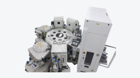
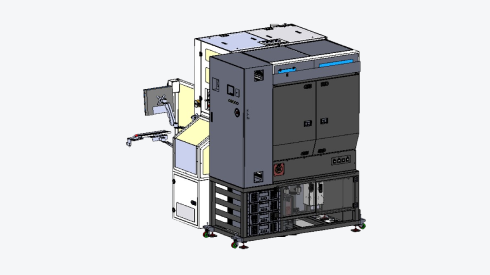
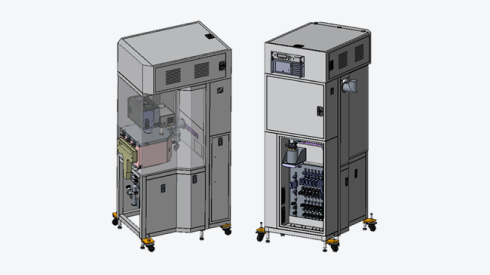
Descum System
KORONA™ DSC200
- Semiconductor Descum System
- It is a plasma treatment system that removes scums in the lateral walls of the pattern before electroplating, or performs surface modification to improve adhesive power, when forming Bump to be used in Flip Chip Bonding in the wafer.
Technology
- ICP Antenna design technology (high density/low damage plasma)
- Control process uniformity (design optimized pedestal and edge ring)
- Plasma stability (design optimized interior of the chamber)
- Functional Transfer Robot (wafer alignment)
Features
- High etch rate using the helical inductively coupled plasma
- Large Diameter Plasma Reactor and Optimized Chamber Inner Structure
- Easy to control process uniformity
- Minimized the CoC (Cost of Consumables)
Specification
- Helical Resonance ICP Plasma(27.12MHz)
(Ion Density: >1E12 cm-3 , Electron Temperature < 1eV) - Cooling Pedestal: 0 ~ 40°C
- Composed of minimized layout(foot print) of 2 independent chambers
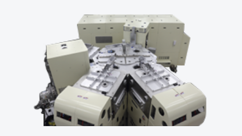
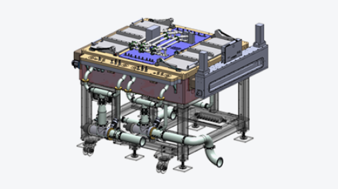
Thin Film Encapsulation
KORONA™ TFE System
- Film structure deposition for the sealant to prevent oxygen and moisture penetration into AMOLED device
- It can be applied to maximum size of Generation 6, 2 Partition board
- Flexible sealant deposition to realize Flexible, rollable, and foldable display
Technology
- ALD (Atomic Layer Deposition) of Multi-linear Nozzle
- Highly clean film deposition technology through in-situ cleaning and gas flow control technology
- Stress control and water vapor permeability optimization technology through multi-layer film design technology
Features
- ICP antenna design technology (high density/low damage plasma)
- Susceptor design technology (possible to remove polymer at the back side and prevent bending of the wafer)
- Pre-Heating (Halogen Lamp) control and process technology
- Functional Transfer Robot (Wafer Alignment)
Specification
| Substrate Loading | Generation 6, 2 Partition, 925mm x 1500 mm |
|---|---|
| Board Temperature | Max. 90℃ |
| Water Vapor Permeability | <5e-5 g/m²/day @ 1000Å, SiNx/SiOx multi-layer structure |
| Film Thickness Uniformity | < 5% |
| Light Transmittance | >90% @ all the ranges of visible light |
| Stress | <±100 MPa |
KORONATM ALD
(Plasma Enhanced Atomic Layer Deposition System)
- KORONATM ALD can be deposited in a low temperature compared to thermal ALD by using plasma
- Application : Active layer, Buffer layer, Encapsulation layer
Technology
- Large area deposition system using plasma scanning
- Large area deposition system using gas nozzles
- Large area deposition system using laminar flow & showerhead
Features
- Good step coverage
- Long PM period
- High deposition rate
- High density thin film
- High throughput
Specification
| System Configuration | 1 Process Chamber(2 Reactor) |
|---|---|
| 2 Slot Loadlock(Semi Auto Loading) | |
| Substrate Size | 730 X 920mm |
| Film Uniformity | <±3% |
| Sub. temperature | 25℃ ~ 250℃ |
| Process Pressure | 1 ~ 10 torr |
| Precursor Source | TMA, DEZ, DIPAS, DADI, TEGa, O2, Ar, N2, H2O… |
| Foot print | 1200(W)*4500(L)*2400(H) |
| Deposition | ALD(Atomic Layer Deposition) - Plasma function included |
| Control | PC Control |
KORONATM CVD
(Plasma Enhanced Chemical Vapor Deposition System)
- Thin film encapsulation deposition system for Micro-OLED
Technology
- Thin film encapsulation layer deposition at low temperature (80℃)
→ Minimized OLED device damage - Excellent WVTR of SiNx & SiON → Minimized thickness of encapsulation layer
- Applied RPS(Remote Plasma System) cleaning
Features
- Excellent thickness uniformity of thin film
- Mask align
- RPS(Remote Plasma System) Cleaning
Specification
| Item | Specification | |
|---|---|---|
| Hardware | Substrate | 8 inch, 12 inch Wafer (EE : 3mm) 200 x 200mm Glass |
| Plasma source | CCP type | |
| RF generator | 13.56 MHz, 1.1 kW | |
| Substrate temperature | 80℃ ± 2℃ | |
| Base pressure | ≤ 1E-3 Torr (TBD) | |
| Process gas | SiH4, NH3, N2O, N2, H2 | |
| In-situ cleaning gas | NF3, Ar | |
| Process | Deposition material | SiNx, SiOx, SiON |
| Deposition rate | ≥3000Å/min | |
| Thickness uniformity | ≤ ± 3% | |
| Stress | ≤ ± 100 MPa | |
| WVTR | ≤ 5E-4 g/m²/day @ SiNx 1μm | |
| ≤ 5E-4 g/m²/day @ SiON 1μm | ||
| ≤ 1E-3 g/m²/day @ SiOx 1μm | ||